Phillip. I think this guy might be on LPF too.
I sent a PM for the prices he offered.
Edit: Received an answer, prices look good. I asked him if I can post the prices he is offering me here, sometimes prices offered to hobbyists differ from their regular price and if so, I won’t post here.
Huh. I actually know Phillip! He’s from Austria, is the CEO of a (smaller) company there. Very nice guy, I got my pump diode from him. His prices are very reasonable indeed.
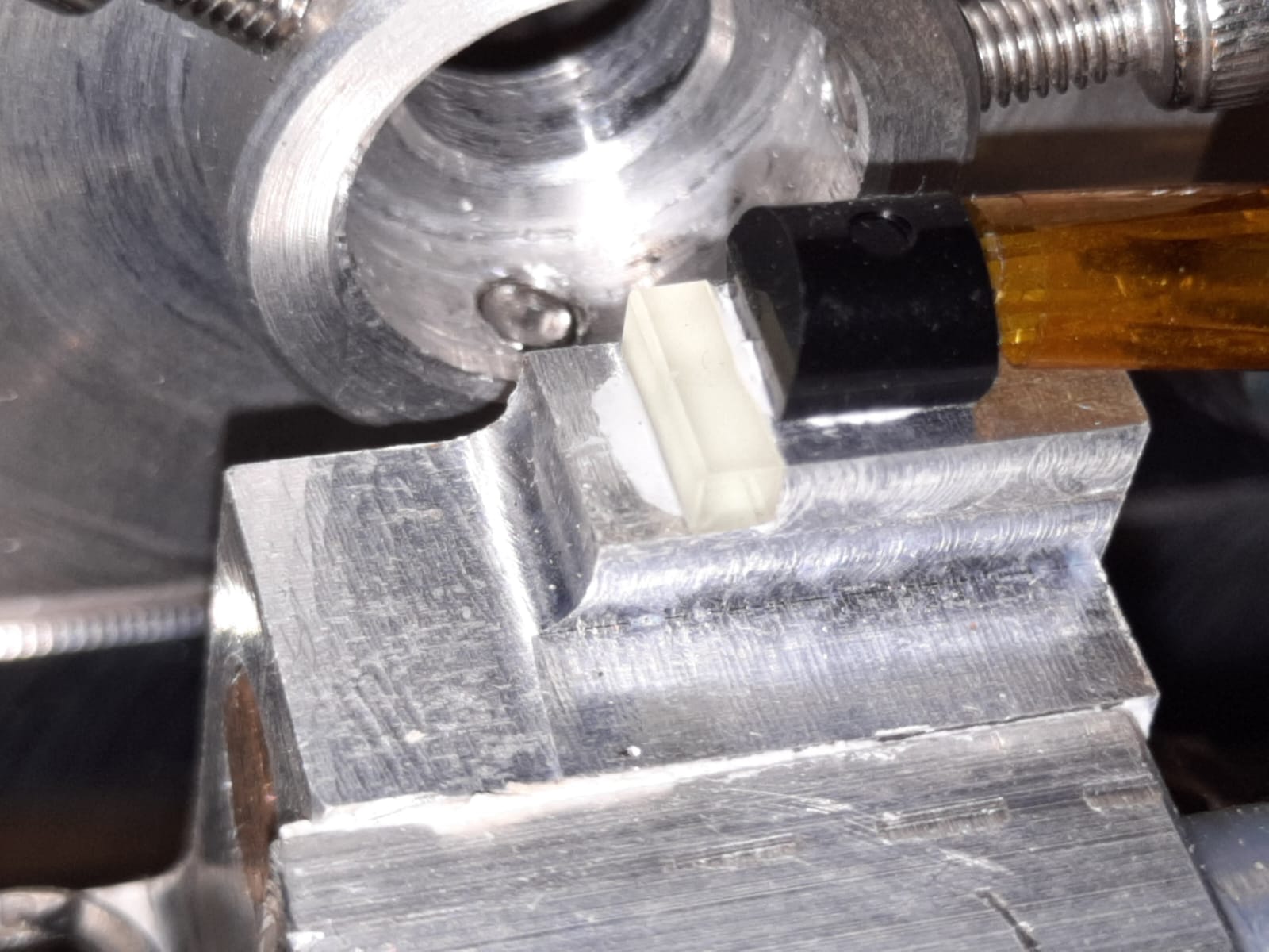
Here’s the photo of the crystal, as I said its 2x2x6mm. The black block next to it is a TO-92 packaged LM35 temperature sensor. I used a very small amount of thermal glue to fix it in place. Indium foil or something like that is better but at my pump powers crystal overheating was not a problem.
Very cool. And thanks for the photo. Chris will be happy. Unfortunately I’m about to get some shut eye now. But thanks. I like the idea of a temp sensor.
As for Phillip he does seem like a friendly and helpful guy.
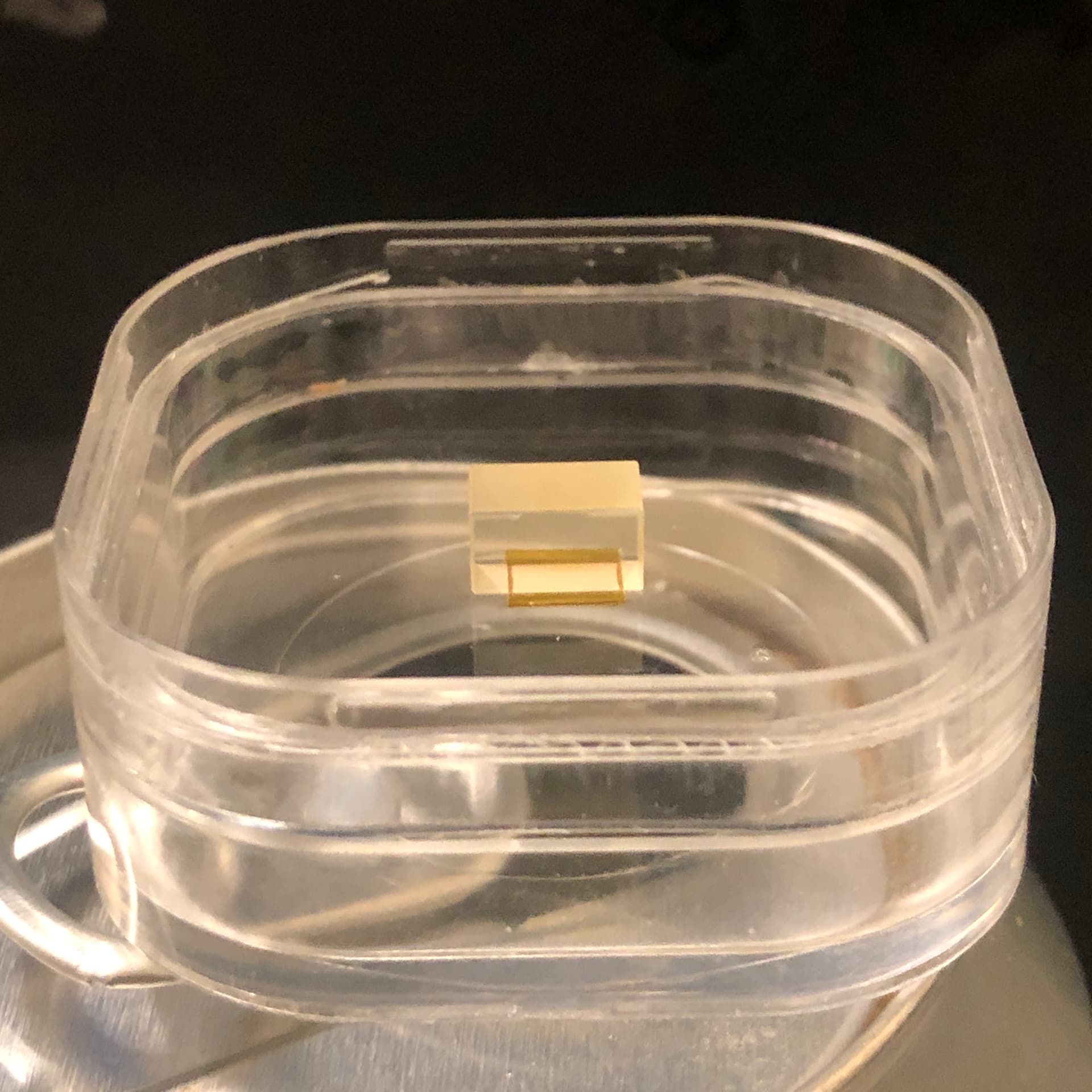
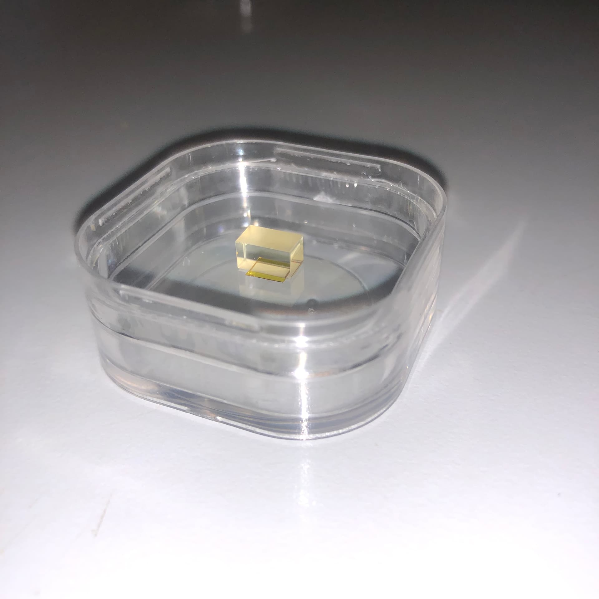
Beautiful crystal! I am very much looking forward to seeing it lase ![]()
I have been thinking - on and off - about a building a laserpointer out of my crystal and optics, even though I don’t really need it. Would be an interesting challenge though.
We’re currently working on that challenge now. It is rather challenging to say the least. A lot of thought has had to go into this project. But we’re making good progress. We’re using wavelength selected NUBM44’s so I am currently trying to get the best focal match for the crystal. I’ve been doing a lot surrounding the optical side. And building stuff has been working on the electronics. And Chris has been ordering and sourcing parts.
We are predominantly working on 607nm.
Hi guys, I have now finished the report for the Pr:YLF project, you can find it here. I was able to measure the output powers of the setup at my uni so the power measurements are reliable. The pump diode (most likely) showed weird behaviour above 600mW of pump power, degrading the output powers above this threshold, so the maximum power were not as high as the setup likely can do, see the report for more info.
Also, I had to align the mirrors in their lab with limited time, so that might have been another factor.
Nice work.
I found a typing mistake.
First page last sentence:
for the pumplight and high reflectivity for 523 nm iss installed
I find the output power anomaly quite interesting.
At which temperature should your diode reach 444nm @ 1,5A?
I would think temperature is a big factor.
You ruled that out but did not explain how.
I could also imagine that the thermal lensing is a problem. Your method of only bonding one side of the crystal your heatsink would introduce uneven thermal expansion because the path length from the hot spot to heatsink is different in each direction. So you would get a uneven, non spherical (not even close) expansion and therefore thermal lens.
But i would think that should be reflected at the output spot.
Does get deformed / switch to a different TM / show more random splash outside the center spot with increasing pump power?
Also the thermal mass of the crystal is so low and the input power so high that you most likely won’t notice a “slow” change in output power while something is heating up.
Thank you, corrected the mistake.
Yes, I also find it quite odd. The temperature should be around 25°C at 1,5A but the temperature related wavelength shift of InGaN diodes is quite small, so it does not matter that much.
Thermal lensing might be an issue but I find it hard to believe that it is the main culprit. I actually bonded the cystal on two sides, but more importantly, can measure the temperature using the sensor directly next to it. Its temperature barely changes at all during operation, maybe 1-2°C. Also, I don’t think it explains why I can run it at 550mW no problem for a long time but as soon as I get to 600mW-650mW it degrades.
I did actually measure the diode at <500 mW using the professional laser power meter, but couldn’t measure beyond that since the sensor head allows 500mW max. I extrapolated the output power from the current beyond 500mW, assuming linear behaviour (which was very accurate for <500mW).
However I did get to calibrate my own power meter which uses a small TEC and a big heatsink so I could (and will) characterize the diode beyond 500mW to see whether its output power drops. Also, I’ll look at the far field of the diode to look at the TEM structure, which is my main suspect currently. I haven’t gotten around to doing that yet, I did the power measurements yesterday ![]()
Some Osram diodes state the thermal restance between die and case of the diode. A similar 1,6W diode got 15k/W
So for 5W power dissipation the die will get 75k hotter than the case.
Even at the low shift of blue/greed diodes, that will produce some shift.
Your sensor is thermally far away from your crystal and diode.
Its mechanically close but not thermally.
So crystal temp and diode temp could be a problem.
Measuring the diodes output will give useful data.
My experience is: the emitting area of the diode willl get bigger with increasing current but not as much to make a real difference.
I estimated some resistances.
You can see how your sensor is actually thermal far away from the stuf you try to measure.
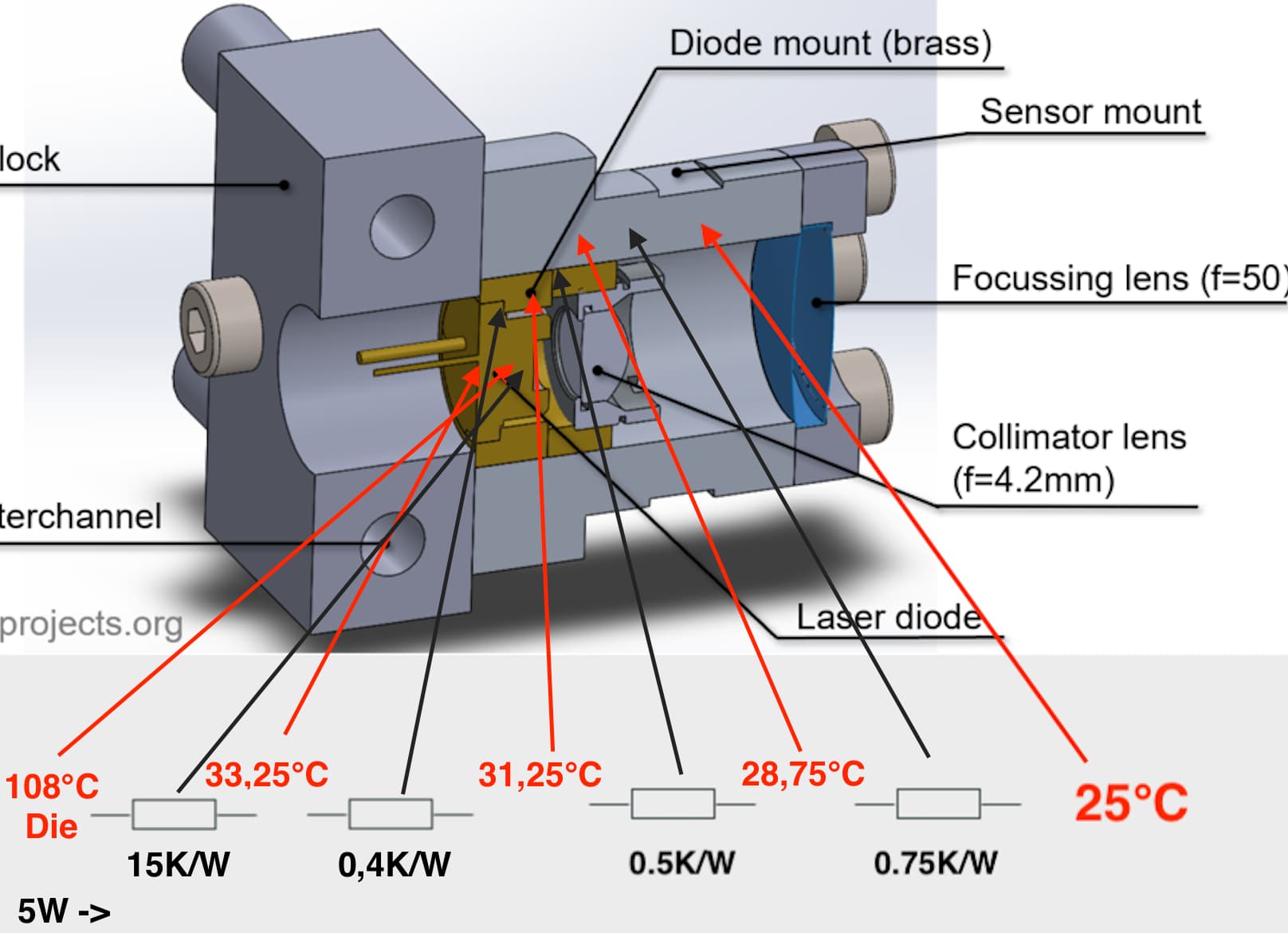
If you now think about how your sensor is actually also thermally connected to the air and its wires.
Also you are not cooling with your sensor, so most of the heat is actually flowing in the direction of the water block which is better connected to the sensor than your diode.
Each material interface is thermally bad. Your sensor just has one interface to the water block. So its actually worse than my diagram.
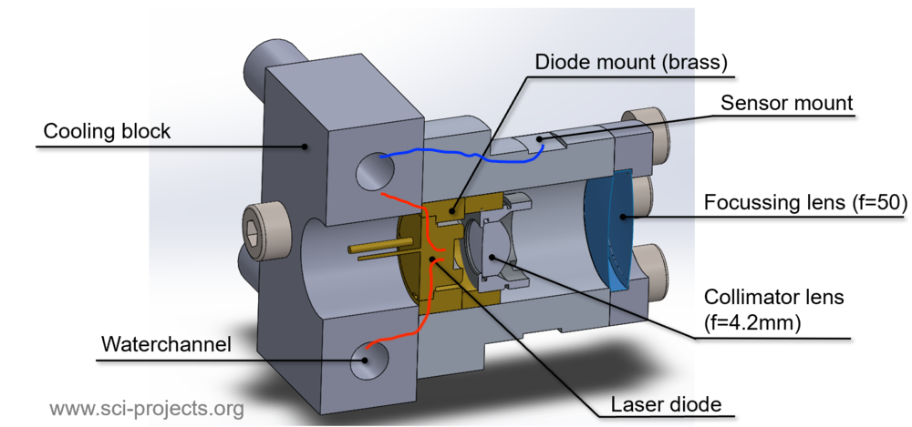
The blue path might have a higher resistance than the red path but there is almost no heat load on your blue path. So it will measure closer to your water temperature than the diode temperature.
Depending on how good the thermal connection between the brass holder and the round lens holder is, most of the diode dissipation would flow trough the upper red path. Which has two interfaces and worse material (brass is soo good). It will produce temperature drop across the thermal resistance but the sensor won’t really see the drop as its better connected to the water block.
Which software did you use to make the cad drawing? Fusion360 (free for students) can do thermal simulations.
Thank you for your detailled explanation. I will try to measure the diodes temperature directly using a thermocouple when I characterize the diode. Thermal management really seems to be my nemesis ![]() Well, we’ll see.
Well, we’ll see.
Btw. the diode, its holder and the lens holder are fixed using light interference fits.
For the CAD drawing I used SolidWorks since I currently have a student license and am familiar with it (also with the simulation part, but I didn’t actually do that). I am familiar with Fusion, since I use it regularly for CAM, but I haven’t used its simulation features.
Nothing to worry about.
Its difficult to estimate stuff like that. It all depends on surface finishes. A rough milled surface with high Ra will have a very high thermal resistance while low Ra finishing tool paths are very good.
Might also be that I am overthinking that a little bit and your problem comes from something completely different.
Take a look at fusion, I can very much recommend it in regards to its thermal simulation capability. Its very easy to use and can give you an intuitive sense of what’s going on if you spend a little time simulating different scenarios.
So I finally took the time to look at the beam shape of the diode. I removed the mirrors crystals and looked at the shape about 200mm away:
https://youtube.com/shorts/CSoDuNCHm9c
Sorry, don’t know how to embed YT Videos… I think it is pretty clear that the beam shape changes around 500-600mW. I am not sure if that is the reason for the decline in power but I would be a pretty big coincident I think.
EDIT: While testing I also got this “doughnut” mode when the resonator was adjusted right between TEM00 and TEM01:
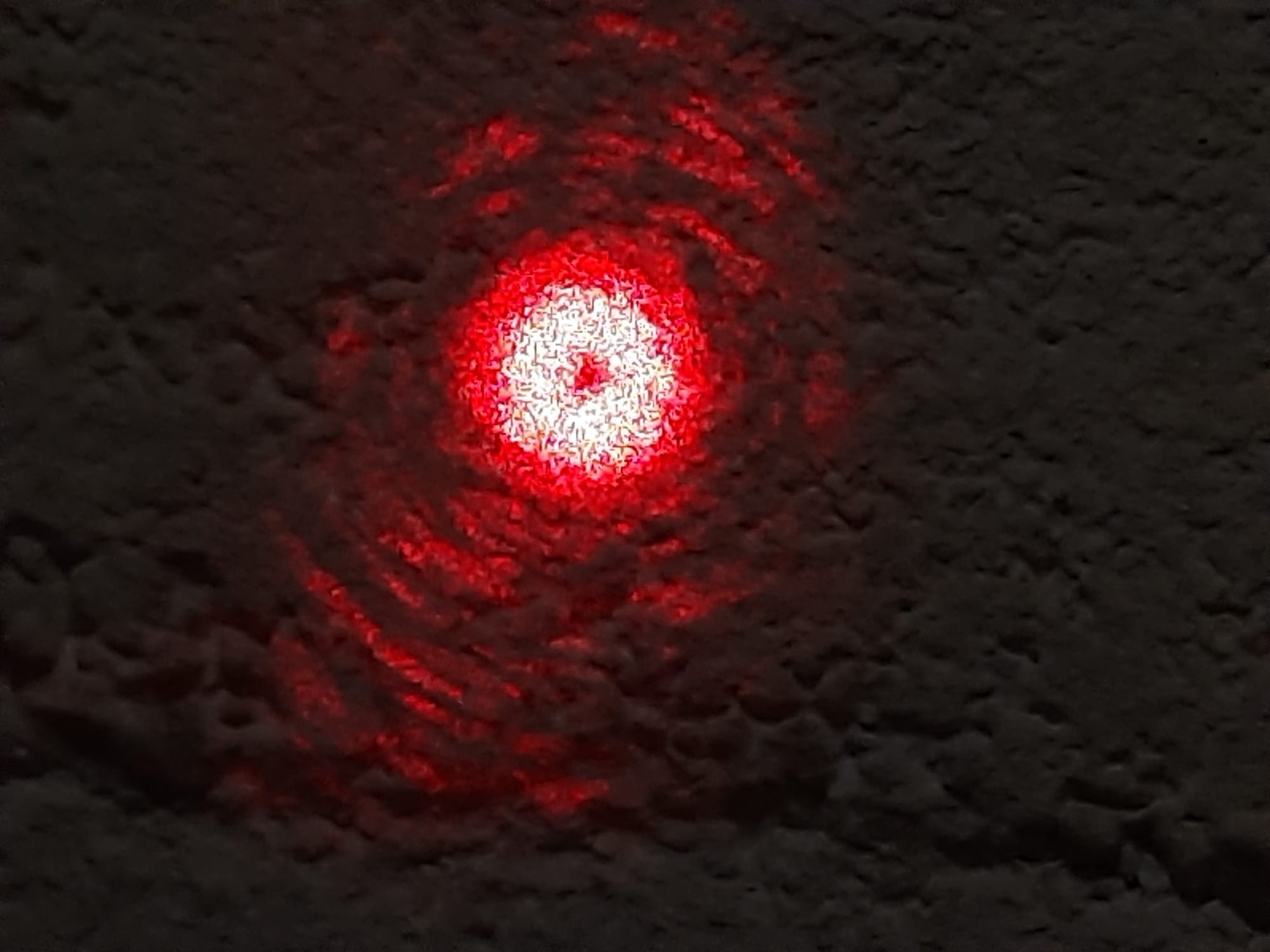
Not really useful but pretty interesting nonetheless, I think.
Very Interesting. Looks like the beam gets wider, so more modes begin to lase.
I would have thought that the power would increase. It might be that the outer mode competes with the inner mode and reduces the power it. Leaving you with lower power in the overlapping region.
So if my assumption is correct, driving the diode even harder should eventually increase the output power.
Yes, I agree with your assumption regarding the modes. Another way would probably be better pump shaping so that the overlap at >600mW is good. I suppose under 600mW the efficiency would then be pretty poor but if I had to choose, I’d gladly take that for higher max output powers ![]() But pump shaping for this module is currently (time-wise) not possible for me. Maybe next year.
But pump shaping for this module is currently (time-wise) not possible for me. Maybe next year.